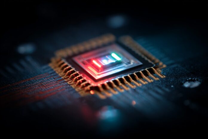
The world of computing is on the brink of a transformative leap. Photonic chips, which harness light rather than electrons for data movement, could transform both speed and energy efficiency across industries. Most importantly, emerging research now shows that integrating quantum dot lasers directly on silicon may finally solve a decades-old challenge. Because this innovation bridges a crucial gap in photonic chip design, it promises not only enhanced performance but also affordability and scalability — two factors critical for mass production.
Moreover, this breakthrough is set to redefine data center architectures along with everyday consumer technology. Therefore, the integration of lasers within silicon-based platforms offers significant advantages over traditional electronic chips. Besides that, as more researchers worldwide join in these efforts, the future of integrated photonics appears brighter than ever.
Why Photonic Chips Have Lagged Behind
Traditional silicon chips operate by moving electrons through circuits, which inherently limits speed and energy efficiency as the data load increases. Because photonic chips rely on light to transmit information, they inherently overcome many of the bottlenecks experienced by electron-based systems. Most importantly, light travels faster and with less resistance, making photonic chips attractive for next-generation applications.
However, the pitfall has always been the integration of laser components. The materials required for high-performance lasers, such as III-V semiconductors, were incompatible with silicon, creating significant technical hurdles. This incompatibility led to premature efforts that resulted in poor performance, increased errors, and ultimately high production costs. Consequently, breaking these barriers has been a major focus for teams around the globe, including those highlighted by UC researchers.
The Quantum Dot Laser Breakthrough
Researchers at the University of California have successfully integrated quantum dot lasers directly onto silicon photonic chips using a multi-step growth technique. This process, which combines metalorganic chemical vapor deposition and molecular beam epitaxy, creates a crystalline laser layer that bonds seamlessly with the silicon substrate. Because the laser is built right into the chip, issues like optical beam spread and signal loss are significantly reduced.
In addition, filling the laser gap with specialized polymers has led to a “pocket laser” design that is both durable and efficient. For instance, these quantum dot lasers have demonstrated the ability to withstand high temperatures for over six years while retaining optimal optical performance. Most importantly, this new method addresses previous manufacturing challenges by ensuring that laser integration does not require a complete overhaul of existing fabrication processes, as further discussed in recent reports.
Cost, Speed, and Manufacturing Advantages
This breakthrough method tackles one of the most expensive barriers in photonic chip production: achieving seamless, low-loss coupling with silicon. Because the quantum dot lasers are grown directly on the chip, traditional issues such as defects at the laser-silicon interface, which previously led to energy loss or even device failure, are minimized considerably. Therefore, this approach simplifies the manufacturing process by utilizing existing silicon CMOS production lines. Most importantly, the reduction in defects makes the chips not only more reliable but also more scalable for mass production.
Because the integration process is both compatible with and adaptable to conventional manufacturing techniques, it paves the way for high-yield production. Transitioning from a lab-based prototype to a production-ready solution means that industries can now envision affordable photonic chips powering data centers, mobile devices, and more. This is a significant step toward integrating photonics fully into our everyday technology.
Applications: From Data Centers to Everyday Devices
The benefits of this innovation extend far beyond the manufacturing floor. In data centers, the increase in bandwidth and decrease in power consumption provided by these new photonic chips can revolutionize network efficiency. This is because the direct integration of quantum dot lasers on silicon allows for ultra-fast data transfer while simultaneously minimizing the energy required for operation.
Moreover, consumer electronics such as smartphones, wearables, and laptops stand to gain enormously. With improved energy efficiency and rapid data processing capabilities, devices can be made more powerful without compromising battery life. As highlighted by various research articles, including those on SciTechDaily, this technology is poised to accelerate the mainstream adoption of photonics in everyday gadgets.
A Step Towards Fully Integrated Photonics
One of the long-standing challenges in photonics has been integrating an electrically pumped light source with silicon. Recent advances have demonstrated that using group IV elements, such as silicon-germanium-tin, might provide a pathway to achieve this integration efficiently. Most importantly, these innovations represent the final puzzle piece in making photonic integrated circuits as routine and cost-effective as electronic circuits.
Furthermore, by unlocking the ability to integrate laser sources directly into the chip, another door opens for innovations in quantum computing and other high-speed applications. Because electrically pumped lasers are now becoming a reality, they herald a new era of ultra-fast, low-power computing solutions that could reshape technology as we know it.
The Road Ahead: Lower Power, Higher Speed, and Mass Adoption
Looking forward, the future of photonic chips is filled with promise. Because ongoing research continues to refine waveguide designs and boost output power, we are likely to witness further increments in performance. Transitioning from prototype to commercial products will help meet the increasing demand in data centers, cloud computing, and artificial intelligence (AI) applications.
Additionally, the broader adoption of these technologies will facilitate collaborative advances in related fields, including integrated circuit design and quantum computing. Therefore, the advent of photonic chips with on-chip lasers marks a significant turning point—where high-speed data processing, lower power consumption, and mass production converge. For further details on high-power tunable lasers reshaping the industry, visit Syntec Optics.
Conclusion: A New Era for Photonic Integration
In summary, the integration of quantum dot lasers on silicon is set to revolutionize the field of photonics. Because researchers have overcome the longstanding material incompatibility issues, the path is now clear for photonic chips to become a viable and cost-effective alternative to their electronic counterparts. Most importantly, this breakthrough is not just a technical achievement but a promise of faster, more energy-efficient, and scalable computing solutions.
As these methods continue to evolve and mature, we are likely to see photonic chips powering data centers, enhancing consumer electronics, and possibly even paving the way for the next generation of quantum computing. Ultimately, this progress heralds a future where photonic technology meets the mass production standards required for global adoption.


